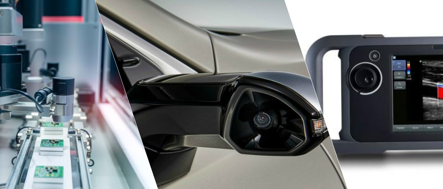
Introduction
Most camera hardware failures trace back not to optics or firmware, but to a single upstream decision: choosing the wrong CMOS image sensor for the application. The global CMOS image sensor market is projected to reach USD 26.9 billion by 2026, driven by automotive, medical, and machine vision demand, yet many engineering teams still approach camera sensor selection with criteria borrowed from the consumer smartphone playbook. That approach rarely survives contact with industrial field conditions, automotive regulatory requirements, or the power constraints of an embedded vision system.
Sony, OmniVision, and ON Semiconductor dominate three distinct segments of this market, each optimized for different performance vectors. Understanding where each manufacturer’s architecture excels, and where it fails, is the starting point for any defensible camera sensor selection decision.
How the CMOS Image Sensor Market Is Actually Segmented
The three-way competition between Sony, OmniVision, and ON Semiconductor is not a straightforward horse race. Each company has spent a decade engineering its CMOS image sensor portfolio around specific market realities, and their market positions reflect those choices.
Sony currently holds approximately 42% of the global CMOS image sensor market. Its dominance comes from a vertically integrated manufacturing model. As an IDM (Integrated Device Manufacturer), Sony controls silicon fabrication, packaging, and process node development in-house. This allows it to iterate on pixel architecture faster than fabless competitors and deploy technologies like back-illuminated sensing and three-layer stacked CMOS at scale before the rest of the industry catches up.
Samsung holds around 19% market share with a different structural advantage: it is a comprehensive semiconductor conglomerate. Its ISOCELL pixel isolation technology, first introduced in 2013, gave Samsung a competitive pixel density path independent of Sony’s stacked architecture. Samsung has since pushed pixel pitch from 1.0 micrometers in 2015 down to 0.7 micrometers by 2018, with a roadmap extending toward 0.56 micrometers. For camera sensor selection in flagship consumer devices, Samsung presents a credible alternative to Sony, particularly for teams already integrated into Samsung’s broader supply chain.
OmniVision sits at approximately 11% global market share. Once the market leader prior to 2011, the company lost ground to Sony and Samsung in the smartphone segment but retained a technically sophisticated product line. Today, OmniVision’s most defensible position is in automotive CMOS image sensors, medical endoscopy, and surveillance, all markets where pixel density is less critical than functional safety, low-light performance, and miniaturization. In 2021, OmniVision’s automotive CMOS image sensor revenue reached approximately RMB 2.3 billion, representing roughly 85% year-over-year growth.
ON Semiconductor (onsemi) operates differently from all three. Rather than competing in the high-volume consumer segment, onsemi has concentrated its CMOS image sensor development on automotive ADAS, industrial machine vision, and medical imaging where radiation hardness, wide dynamic range, and long product lifecycle availability matter more than pixel count. Its AR0820AT and Hyperlux sensor families are calibrated for precisely this use case. For engineering teams doing camera sensor selection for embedded or autonomous systems, onsemi is often the operationally safer choice even if it rarely appears in consumer benchmarks.
Build the Right Camera System the First Time?
Sony CMOS Image Sensors
Pixel Architecture and Stacking Technology
Sony’s competitive position in CMOS image sensor technology rests on two successive architectural breakthroughs. The first is back-illuminated sensing (BSI), which flips the traditional sensor structure so that photodiodes face the incoming light directly, improving quantum efficiency particularly in low-light conditions. The second is three-layer stacked CMOS, introduced commercially with the IMX400 in 2017, which added a dedicated DRAM layer to enable high-speed burst readout without the rolling shutter artifacts that plague standard sensor designs.
Sony further extended this with its dual-layer transistor pixel stacking architecture. This approach separates photodiode and pixel transistor layers, allowing each to be independently optimized. The result is better signal-to-noise ratio at smaller pixel pitches, which matters in applications where the sensor footprint is constrained but image quality cannot be compromised. Sony’s roadmap has moved from 0.8 micrometers (IMX586, 2018) to 0.7 micrometers (IMX758) in a four-year span.
Where Sony CMOS Sensors Perform Well
Sony CMOS image sensor products are the logical default for premium consumer electronics, broadcast cameras, and any application where low-light sensitivity and color fidelity at small pixel pitch are the dominant requirements. Sony’s sensor supply position in the iPhone ecosystem illustrates the level of integration its technology supports.
For camera sensor selection in security cameras and surveillance systems with demanding nighttime imaging requirements, Sony sensors are frequently the first evaluation unit on the bench. Their full-well capacity, noise floor, and ISP compatibility tend to outperform alternatives in these conditions.
Where Sony CMOS Sensors Fall Short
Sony’s fabless competitors in automotive and industrial applications often outperform it on functional safety compliance, extended temperature range, and long-term supply commitment. Sony’s automotive CMOS image sensor expansion is relatively recent, and its automotive qualification track record is shorter than onsemi’s. Teams doing camera sensor selection for ISO 26262 ASIL-rated systems should assess Sony’s automotive-grade offerings carefully against alternatives with longer field deployment histories.
OmniVision
Structural Position and Manufacturing Dependencies
OmniVision is a fabless CMOS image sensor manufacturer, which means it relies on TSMC and other foundries for silicon production. This creates a structural constraint in technology iteration speed compared to Sony’s IDM model. However, it also means OmniVision can leverage TSMC’s process node advances and allocate engineering resources toward sensor architecture rather than fab operations.
The tradeoff becomes visible in the camera sensor selection process for high-volume applications: OmniVision can move quickly on product definition but faces tighter foundry capacity constraints than vertically integrated competitors during supply crunches.
Medical and Endoscopy Applications
OmniVision’s strongest differentiator in CMOS image sensor development is its sub-millimeter endoscopy sensor line. The global endoscope market grew at roughly 30% between 2018 and 2023. OmniVision’s OVMed sensor series targets disposable endoscopes, capsule endoscopes, and catheter-based imaging, all use cases where the sensor die must fit in an extreme form factor without sacrificing image quality.
Any camera sensor selection exercise for medical imaging devices with space constraints under five millimeters should include OmniVision’s catalog as a primary reference. The company’s pixel-on-chip architecture allows it to integrate ISP functions directly onto the sensor die, reducing system complexity in form-factor-limited designs.
Automotive Imaging Traction
OmniVision’s automotive CMOS image sensor portfolio supports ADAS, surround view, and in-cabin driver monitoring applications. Its customer list includes Tesla, BYD, Geely, Volkswagen, Toyota, Honda, BMW, and Mercedes-Benz, which reflects genuine automotive-grade qualification across multiple tier-1 ecosystems. The localization advantage OmniVision built during China’s domestic semiconductor substitution period from 2018 onward gave it a supply chain position with Chinese OEMs that Sony and onsemi have been slower to develop.
ON Semiconductor
Why Onsemi Approaches Camera Sensor Selection Differently
ON Semiconductor does not compete primarily on pixel count or consumer photography metrics. Its CMOS image sensor strategy centers on wide dynamic range, global shutter accuracy, high frame rate operation, and long-term part availability commitments that industrial and automotive customers require. These requirements are structurally different from what drives smartphone sensor development, and onsemi has engineered its roadmap accordingly.
For any camera sensor selection exercise in machine vision, autonomous driving, or industrial inspection, onsemi’s AR-series sensors consistently appear on the shortlist. The AR0820AT, for example, delivers 8.3 megapixels with high dynamic range and a thermal operating range suited to automotive underhood and exterior environments.
Global Shutter vs. Rolling Shutter in Camera Sensor Selection
This is a decision point that frequently determines whether Sony or onsemi wins a camera sensor selection evaluation in machine vision. Sony’s stacked sensors use rolling shutter readout, which introduces image distortion when capturing fast-moving objects. Onsemi’s global shutter CMOS image sensor products read all pixels simultaneously, eliminating motion artifacts entirely.
Applications like barcode scanning at high conveyor speeds, PCB inspection, robotics end-of-arm tooling, and traffic enforcement cameras require global shutter. OmniVision and Sony offer limited global shutter options in their standard catalogs. Onsemi’s product depth in this category makes it the default choice when global shutter is a firm requirement in the camera sensor selection criteria.
Hyperlux and Next-Generation Low-Light Performance
Onsemi’s Hyperlux CMOS image sensor family targets automotive exterior cameras operating in low ambient light, a condition common at dawn, dusk, and in tunnel approaches. Hyperlux achieves low-light performance through larger pixel pitch and optimized well capacity rather than computational post-processing. This matters because camera sensor selection for ADAS applications cannot rely on software compensation for sensor photon capture deficiency. The photon must be collected, not synthesized.
Head-to-Head Camera Sensor Selection Criteria Across Key Parameters
| Parameter | Sony Semiconductor Solutions | OmniVision Technologies | onsemi |
|---|---|---|---|
| Best Known For | Low-light imaging | Automotive & medical cameras | Industrial & ADAS vision |
| Sensor Strength | BSI and stacked CMOS | Compact HDR designs | Global shutter & HDR |
| Low-Light Performance | Excellent | Very good | Strong in harsh conditions |
| Global Shutter | Limited | Limited | Extensive support |
| Ideal Applications | Surveillance, consumer cameras | Automotive, medical | Robotics, machine vision |
| Long-Term Availability | Moderate | Moderate | Excellent |
| Integration Ease | Easier ISP ecosystem | Flexible integration | Requires deeper tuning expertise |
Pixel Architecture and Low-Light Sensitivity
Sony leads in pixel pitch miniaturization and BSI efficiency for small-pixel designs. OmniVision delivers competitive low-light performance in its automotive and medical lines through pixel architecture optimization rather than pixel count maximization. Onsemi’s larger pixel approach in Hyperlux trades pixel density for fundamental photon collection efficiency. The right CMOS image sensor choice depends on whether the application requires maximum resolution within a fixed optical format or maximum photon sensitivity within a fixed illumination budget.
Dynamic Range Requirements
For automotive surround view and machine vision applications where scenes include both direct sunlight and deep shadow simultaneously, onsemi’s CMOS image sensor products consistently deliver higher native dynamic range figures than Sony’s comparable sensors. OmniVision’s automotive sensors offer HDR modes, but the architecture differs from onsemi’s native wide dynamic range implementation. Teams doing camera sensor selection for outdoor fixed cameras or automotive exterior applications should treat dynamic range as a first-order evaluation criterion, not a secondary specification.
Supply Chain Resilience and Long-Term Availability
Sony prioritizes high-volume consumer segments in capacity allocation. During shortage periods, automotive and industrial customers regularly experience allocation constraints on Sony’s CMOS image sensor products. Onsemi explicitly commits to extended production lifecycle programs for automotive and industrial parts, frequently guaranteeing availability horizons of ten or more years. OmniVision’s dependency on foundry capacity creates its own supply risk profile. Supply chain resilience is a legitimate camera sensor selection criterion that engineering teams often underweight relative to performance specifications.
Functional Safety Certification
For camera sensor selection in ISO 26262 ASIL-B or ASIL-D systems, onsemi’s automotive-grade CMOS image sensor products carry a longer qualification pedigree than Sony’s more recently expanded automotive portfolio. OmniVision has made significant investments in automotive qualification across ADAS applications. All three require careful safety case documentation from the system integrator regardless of sensor choice.
Software Ecosystem and ISP Integration
Sony’s IMX series integrates extensively with major ISP silicon from MediaTek, Qualcomm, and Ambarella. OmniVision publishes detailed ISP tuning guides and maintains active software support for its sensor register maps. Onsemi’s sensors integrate well with automotive SoCs from NXP, Texas Instruments, and Renesas, but require more camera design expertise to tune correctly. For teams without deep ISP firmware capabilities, camera sensor selection should account for the availability of reference tuning data and BSP support from the sensor vendor.
Struggling with Sensor Trade-offs?
The Role of a Camera Design Company in Sensor Selection and Integration
Selecting the right CMOS image sensor resolves only the first layer of a camera development program. Translating a sensor selection into a production-ready camera module requires hardware design, optical integration, firmware development, ISP tuning, and manufacturing validation, all of which have dependencies on the specific sensor’s architecture and electrical interface.

A camera design company with direct engineering experience across Sony, OmniVision, and onsemi sensor families can compress the timeline between camera sensor selection and first production units significantly. This matters because each CMOS image sensor vendor uses different MIPI CSI-2 lane configurations, different I2C register map structures, different power sequencing requirements, and different noise characteristics that affect PCB layout decisions.
Hardware Design Considerations Tied to Sensor Architecture
The physical design of a camera module cannot be decoupled from the CMOS image sensor chosen. Pixel pitch determines the minimum optical format and lens selection. Sensor operating voltage defines power supply rail requirements. Thermal dissipation from the sensor die affects board stackup and housing design. A camera design company that works across multiple sensor families understands these dependencies from direct experience rather than datasheet extrapolation.
Firmware, BSP, and ISP Tuning
Writing a board support package (BSP) for a CMOS image sensor involves mapping the sensor’s register interface to the host processor’s camera interface driver, configuring the MIPI D-PHY timing to match the sensor’s output, and implementing the auto-exposure and auto-white-balance control loops that the sensor’s firmware does not handle internally. Each sensor vendor’s architecture presents different challenges at this layer.
ISP tuning for a specific CMOS image sensor in a specific optical and lighting environment requires characterization data collected from the physical module, not from the sensor datasheet. This means that any camera sensor selection process should include a realistic estimate of the tuning effort required to achieve production image quality, not just the effort to get the sensor to output pixels.
Validation and Production Readiness
Moving a camera module from engineering validation to production requires electrical test coverage for the CMOS image sensor interface, optical quality verification against acceptance criteria, and a manufacturing test strategy that can detect sensor defects without adding prohibitive test cycle time. These requirements apply regardless of whether the sensor is from Sony, OmniVision, or onsemi. A camera design company with production validation experience across sensor families can define these test parameters from existing data rather than building the test framework from scratch.
Conclusion
Sony’s CMOS image sensor products lead in pixel miniaturization, low-light sensitivity, and consumer ecosystem integration. OmniVision delivers strong performance in automotive, medical, and surveillance applications where form factor and specific functional requirements constrain the design space. Onsemi is the technically correct choice for global shutter machine vision, high dynamic range automotive imaging, and applications requiring a decade-long supply commitment.
No single CMOS image sensor vendor wins every camera sensor selection evaluation. The right framework evaluates pixel architecture against the photon budget, dynamic range against the scene contrast requirement, supply chain risk against the product lifecycle, and functional safety compliance against the system safety goal. Applying smartphone sensor selection logic to automotive or industrial applications consistently leads to late-stage redesigns.
Silicon Signals is a camera design company specializing in end-to-end camera module development across Sony, OmniVision, and ON Semiconductor sensor platforms. From camera sensor selection and hardware design through BSP development, ISP tuning, and production validation, Silicon Signals builds camera systems that meet real application requirements, not marketing specifications. Engineering teams working on automotive, medical, or industrial camera programs can engage Silicon Signals at any stage of the development process, from pre-selection sensor evaluation to full camera module production readiness.
