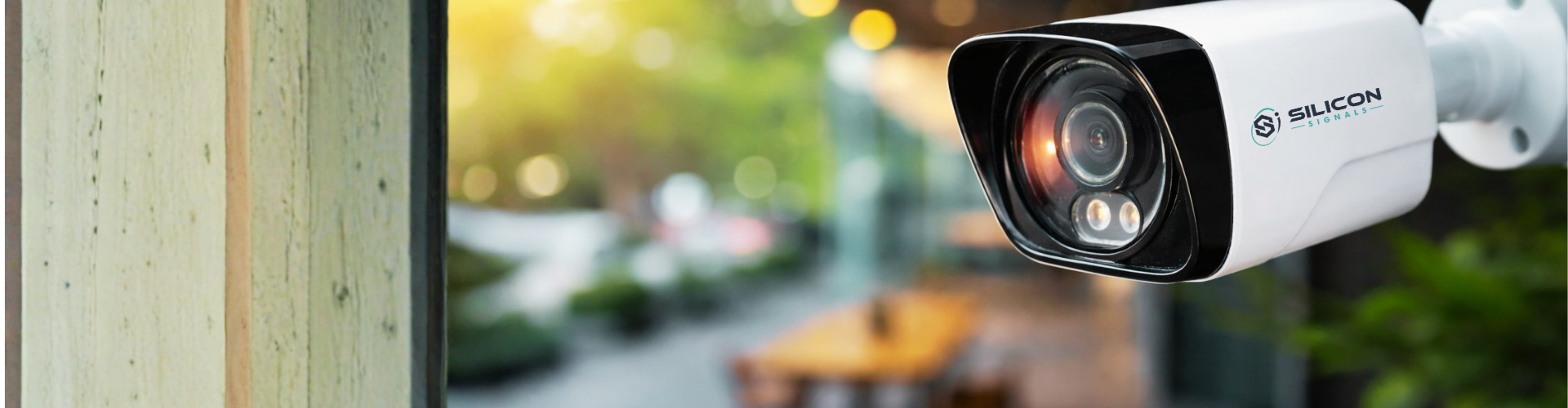
ISP Tuning
What Is ISP Tuning? A Beginner’s Guide
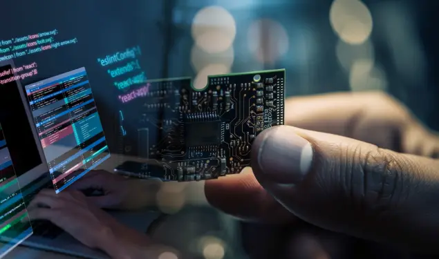
The process of obtaining a high-quality image is not just limited to the camera sensor and lens. Instead, the real processing happens after the light hits the sensor, and the
The process of obtaining a high-quality image is not just limited to the camera sensor and lens. Instead, the real processing happens after the light hits the sensor, and the

From the outside, camera engineering looks easy, but once you get inside, it’s very hard. A camera module isn’t just a lens stuck to a sensor. It is a tightly

From the outside, camera engineering looks easy, but once you get inside, it’s very hard. A camera module isn’t just a lens stuck to a sensor. It is a tightly
From the outside, camera engineering looks easy, but once you get inside, it’s very hard. A camera module isn’t just a lens stuck to a sensor. It is a tightly

From the outside, camera engineering looks easy, but once you get inside, it’s very hard. A camera module isn’t just a lens stuck to a sensor. It is a tightly

From the outside, camera engineering looks easy, but once you get inside, it’s very hard. A camera module isn’t just a lens stuck to a sensor. It is a tightly

The camera is not a secondary consideration if your product relies on vision. It’s the choice. The design of that camera has an impact on image quality, dependability, mechanical fit,
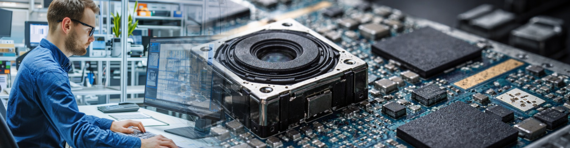
From the outside, camera engineering looks easy, but once you get inside, it’s very hard. A camera module isn’t just a lens stuck to a sensor. It is a tightly
Share Details